TL DD11214
COP688EGCOP684EGCOP888EGCOP884EGCOP988EGCOP984EG
8-Bit
Microcontroller
with
UART
and
Three
Multi-Function
Timers
August 1996
COP688EG COP684EG COP888EG COP884EG
COP988EG COP984EG 8-Bit Microcontroller
with UART and Three Multi-Function Timers
General Description
The COP8
TM
feature family of microcontrollers use an 8-bit
single-chip core architecture fabricated with National Semi-
conductor's
M
2
CMOS
TM
process
technology
The
COP888EG COP884EG are members of this expandable
8-bit core processor family of microcontrollers
(Continued)
Key Features
Y
Full duplex UART
Y
Three 16-bit timers each with two 16-bit registers
supporting
Processor Independent PWM mode
External Event counter mode
Input Capture mode
Y
Quiet design (low radiated emissions)
Y
8k bytes on-board ROM
Y
256 bytes on-board RAM
Additional Peripheral Features
Y
Idle Timer
Y
Multi-Input Wake-Up (MIWU) with optional interrupts (8)
Y
Two analog comparators
Y
WATCHDOG
TM
and clock monitor logic
Y
MICROWIRE PLUS
TM
serial I O
I O Features
Y
Memory mapped I O
Y
Software selectable I O options (TRI-STATE
Output
Push-Pull Output Weak Pull-Up Input High Impedance
Input)
Y
Schmitt trigger inputs on ports G and L
Y
Packages
28 SO or 28 DIP each with 24 I O pins
40 DIP with 36 I O pins
44 PQFP with 40 I O pins
44 PLCC with 40 I O pins
CPU Instruction Set Features
Y
1 ms instruction cycle time
Y
Fourteen multi-source vectored interrupts servicing
External Interrupt with selectable edge
Idle Timer T0
Three Timers (each with 2 Interrupts)
MICROWIRE PLUS
Multi-Input Wake-Up
Software Trap
UART (2)
Default VIS (default interrupt)
Y
Versatile and easy to use instruction set
Y
8-bit Stack Pointer (SP) stack in RAM
Y
Two 8-bit Register Indirect Data Memory Pointers
(B and X)
Fully Static CMOS
Y
Two power saving modes HALT and IDLE
Y
Low current drain (typically
k
1 mA)
Y
Single supply operation 2 5V to 6 0V
Y
Temperature ranges 0 C to
a
70 C
b
40 C to
a
85 C
b
55 C to
a
125 C
Development Support
Y
Emulation and OTP devices
Y
Real time emulation and full program debug offered by
MetaLink Development System
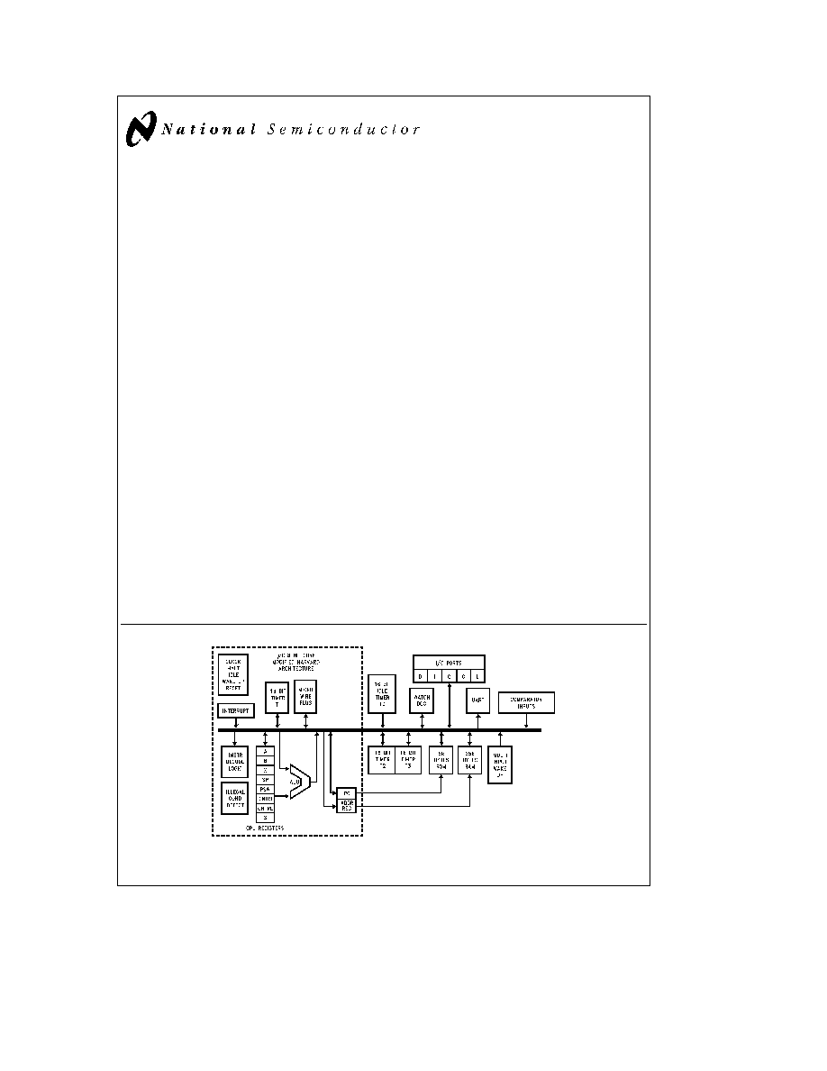
Block Diagram
TL DD 11214 � 1
FIGURE 1 Block Diagram
TRI-STATE
is a registered trademark of National Semiconductor Corporation
MICROWIRE PLUS
TM
M
2
CMOS
TM
COPS
TM
microcontrollers MICROWIRE
TM
and WATCHDOG
TM
are trademarks of National Semiconductor Corporation
IBM
PC
PC-AT
and PC-XT
are registered trademarks of International Business Machines Corporation
iceMASTER
TM
is a trademark of MetaLink Corporation
C1996 National Semiconductor Corporation
RRD-B30M106 Printed in U S A
http
www national com
General Description
(Continued)
They are fully static parts fabricated using double-metal sili-
con gate microCMOS technology Features include an 8-bit
memory mapped architecture MICROWIRE PLUS serial
I O three 16-bit timer counters supporting three modes
(Processor Independent PWM generation External Event
counter and Input Capture mode capabilities) full duplex
UART two comparators and two power savings modes
(HALT and IDLE) both with a multi-sourced wakeup inter-
rupt capability This multi-sourced interrupt capability may
also be used independent of the HALT or IDLE modes
Each I O pin has software selectable configurations The
device operates over a voltage range of 2 5V to 6V High
throughput is achieved with an efficient regular instruction
set operating at a maximum rate of 1 ms per instruction
Low radiated emissions are achieved by gradual turn-on
output drivers and internal I
CC
smoothing filters on the chip
logic and crystal oscillator
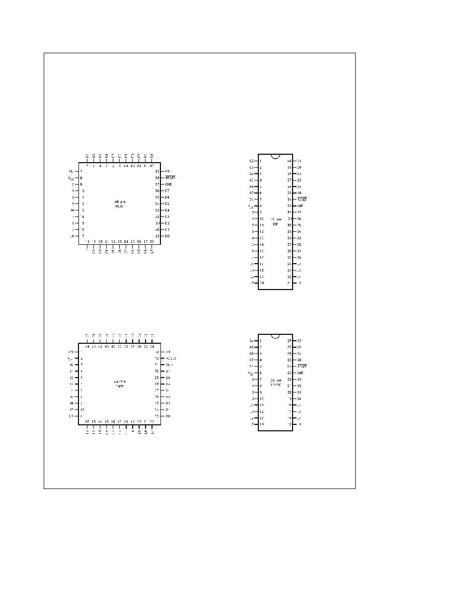
Connection Diagrams
Plastic Chip Carrier
TL DD 11214 � 2
Top View
Order Number COP888EG-XXX V
See NS Plastic Chip Package Number V44A
Dual-In-Line Package
TL DD 11214 � 3
Top View
Order Number COP888EG-XXX N
See NS Molded Package Number N40A
Molded Plastic Quad Flat Package
TL DD 11214 � 30
Top View
Order Number COP888EG-XXX VEJ
See NS Package Number VEJ44A
Dual-In-Line Package
TL DD 11214 � 4
Top View
Order Number COP884EG-XXX WM
or COP884EG-XXX N
See NS Molded Package Number M28B or N28A
FIGURE 2a Connection Diagrams
http
www national com
2
Connection Diagrams
(Continued)
Pinouts for 28- 40- and 44-Pin Packages
Port
Type
Alt Fun
Alt Fun
28-Pin
40-Pin
44-Pin
44-Pin
DIP SO
DIP
PLCC
PQFP
L0
I O
MIWU
11
17
17
11
L1
I O
MIWU
CKX
12
18
18
12
L2
I O
MIWU
TDX
13
19
19
13
L3
I O
MIWU
RDX
14
20
20
14
L4
I O
MIWU
T2A
15
21
25
19
L5
I O
MIWU
T2B
16
22
26
20
L6
I O
MIWU
T3A
17
23
27
21
L7
I O
MIWU
T3B
18
24
28
22
G0
I O
INT
25
35
39
33
G1
WDOUT
26
36
40
34
G2
I O
T1B
27
37
41
35
G3
I O
T1A
28
38
42
36
G4
I O
SO
1
3
3
41
G5
I O
SK
2
4
4
42
G6
I
SI
3
5
5
43
G7
I CKO
HALT Restart
4
6
6
44
D0
O
19
25
29
23
D1
O
20
26
30
24
D2
O
21
27
31
25
D3
O
22
28
32
26
D4
O
29
33
7
D5
O
30
34
8
D6
O
31
35
9
D7
O
32
36
10
I0
I
7
9
9
27
I1
I
COMP1IN
b
8
10
10
28
I2
I
COMP1IN
a
9
11
11
29
I3
I
COMP1OUT
10
12
12
30
I4
I
COMP2IN
b
13
13
3
I5
I
COMP2IN
a
14
14
4
I6
I
COMP2OUT
15
15
5
I7
I
16
16
6
C0
I O
39
43
37
C1
I O
40
44
38
C2
I O
1
1
39
C3
I O
2
2
40
C4
I O
21
15
C5
I O
22
16
C6
I O
23
17
C7
I O
24
18
V
CC
6
8
8
2
GND
23
33
37
31
CKI
5
7
7
1
RESET
24
34
38
32
http
www national com
3
Absolute Maximum Ratings
If Military Aerospace specified devices are required
please contact the National Semiconductor Sales
Office Distributors for availability and specifications
Supply Voltage (V
CC
)
7V
Voltage at Any Pin
b
0 3V to V
CC
a
0 3V
Total Current into V
CC
Pin (Source)
100 mA
Total Current out of GND Pin (Sink)
110 mA
Storage Temperature Range
b
65 C to
a
140 C
Note
Absolute maximum ratings indicate limits beyond
which damage to the device may occur DC and AC electri-
cal specifications are not ensured when operating the de-
vice at absolute maximum ratings
DC Electrical Characteristics
98XEG 0 C
s
T
A
s
a
70 C unless otherwise specified
Parameter
Conditions
Min
Typ
Max
Units
Operating Voltage
COP98XEG
2 5
4 0
V
COP98XEGH
4 0
6 0
V
Power Supply Ripple (Note 1)
Peak-to-Peak
0 1 V
CC
V
Supply Current (Note 2)
CKI
e
10 MHz
V
CC
e
6V t
c
e
1 ms
12 5
mA
CKI
e
4 MHz
V
CC
e
6V t
c
e
2 5 ms
5 5
mA
CKI
e
4 MHz
V
CC
e
4V t
c
e
2 5 ms
2 5
mA
CKI
e
1 MHz
V
CC
e
4V t
c
e
10 ms
1 4
mA
HALT Current (Note 3)
V
CC
e
6V CKI
e
0 MHz
k
0 7
8
m
A
V
CC
e
4V CKI
e
0 MHz
k
0 3
4
m
A
IDLE Current
CKI
e
10 MHz
V
CC
e
6V t
c
e
1 ms
3 5
mA
CKI
e
4 MHz
V
CC
e
6V t
c
e
2 5 ms
2 5
mA
CKI
e
1 MHz
V
CC
e
4V t
c
e
10 ms
0 7
mA
Input Levels
RESET
Logic High
0 8 V
CC
V
Logic Low
0 2 V
CC
V
CKI (External and Crystal Osc Modes)
Logic High
0 7 V
CC
V
Logic Low
0 2 V
CC
V
All Other Inputs
Logic High
0 7 V
CC
V
Logic Low
0 2 V
CC
V
Hi-Z Input Leakage
V
CC
e
6V
b
1
a
1
m
A
Input Pullup Current
V
CC
e
6V V
IN
e
0V
b
40
b
250
m
A
G and L Port Input Hysteresis
0 35 V
CC
V
Output Current Levels
D Outputs
Source
V
CC
e
4V V
OH
e
3 3V
b
0 4
mA
V
CC
e
2 5V V
OH
e
1 8V
b
0 2
mA
Sink
V
CC
e
4V V
OL
e
1V
10
mA
V
CC
e
2 5V V
OL
e
0 4V
2 0
mA
All Others
Source (Weak Pull-Up Mode)
V
CC
e
4V V
OH
e
2 7V
b
10
b
100
m
A
V
CC
e
2 5V V
OH
e
1 8V
b
2 5
b
33
m
A
Source (Push-Pull Mode)
V
CC
e
4V V
OH
e
3 3V
b
0 4
mA
V
CC
e
2 5V V
OH
e
1 8V
b
0 2
mA
Sink (Push-Pull Mode)
V
CC
e
4V V
OL
e
0 4V
1 6
mA
V
CC
e
2 5V V
OL
e
0 4V
0 7
mA
TRI-STATE Leakage
V
CC
e
6 0V
b
1
a
1
m
A
Note 1
Rate of voltage change must be less then 0 5 V ms
Note 2
Supply current is measured after running 2000 cycles with a square wave CKI input CKO open inputs at rails and outputs open
Note 3
The HALT mode will stop CKI from oscillating in the RC and the Crystal configurations Test conditions All inputs tied to V
CC
L and G
0
-G
5
configured as
outputs and set high The D port set to zero The clock monitor and the comparators are disabled
http
www national com
4
DC Electrical Characteristics
98XEG 0 C
s
T
A
s
a
70 C unless otherwise specified (Continued)
Parameter
Conditions
Min
Typ
Max
Units
Allowable Sink Source
Current per Pin
D Outputs (Sink)
15
mA
All others
3
mA
Maximum Input Current
T
A
e
25 C
g
100
mA
without Latchup (Note 5)
RAM Retention Voltage V
r
500 ns Rise
2
V
and Fall Time (Min)
Input Capacitance
7
pF
Load Capacitance on D2
1000
pF
AC Electrical Characteristics
98XEG 0 C
s
T
A
s
a
70 C unless otherwise specified
Parameter
Conditions
Min
Typ
Max
Units
Instruction Cycle Time (t
c
)
4V
s
V
CC
s
6V
1
DC
m
s
Crystal Resonator
2 5V
s
V
CC
k
4V
2 5
DC
m
s
R C Oscillator
4V
s
V
CC
s
6V
3
DC
m
s
2 5V
s
V
CC
k
4V
7 5
DC
m
s
Inputs
t
SETUP
4V
s
V
CC
s
6V
200
ns
2 5V
s
V
CC
k
4V
500
ns
t
HOLD
4V
s
V
CC
s
6V
60
ns
2 5V
s
V
CC
k
4V
150
ns
Output Propagation Delay (Note 6)
R
L
e
2 2k C
L
e
100 pF
t
PD1
t
PD0
SO SK
4V
s
V
CC
s
6V
0 7
m
s
2 5V
s
V
CC
k
4V
1 75
m
s
All Others
4V
s
V
CC
s
6V
1
m
s
2 5V
s
V
CC
k
4V
2 5
m
s
MICROWIRE
TM
Setup Time (t
UWS
)
20
ns
MICROWIRE Hold Time (t
UWH
)
56
ns
MICROWIRE Output Propagation Delay (t
UPD
)
220
ns
Input Pulse Width
Interrupt Input High Time
1
t
c
Interrupt Input Low Time
1
t
c
Timer Input High Time
1
t
c
Timer Input Low Time
1
t
c
Reset Pulse Width
1
m
s
Note 5
Pins G6 and RESET are designed with a high voltage input network for factory testing These pins allow input voltages greater than V
CC
and the pins will
have sink current to V
CC
when biased at voltages greater than V
CC
(the pins do not have source current when biased at a voltage below V
CC
) The effective
resistance to V
CC
is 750X (typical) These two pins will not latch up The voltage at the pins must be limited to less than 14V
Note 6
The output propagation delay is referenced to the end of the instruction cycle where the output change occurs
http
www national com
5